
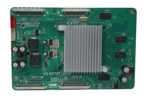


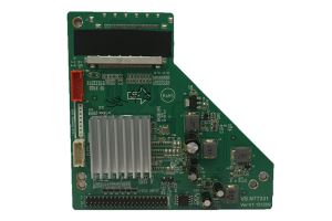
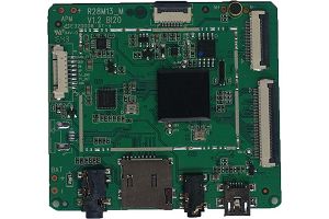
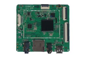
China Design 120 HZ Change to 60Hz TCON Board for Samsung TV 240Hz
-
Payment


-
Origin
China Mainland
-
Minimum Order
1
-
Packing
Pieces
- Contact Now Start Order
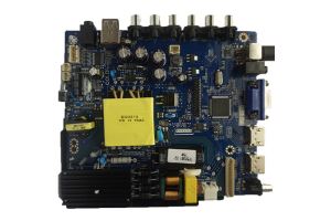
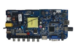
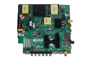
- Description
Product Detail
60HZ change to 120HZ TCON board
VS.NT7213 is a LVDS@60HZ adapter plate / VBY1@60HZ signal to V-BY-One@120HZ signal, using single chip NovateK solutions NT72324BG, LVDS signal input support FHD, support VBY1 4K2K 60HZ signal input, maximum support VBY1 interface, 4K2K@120Hz signal output
1. Product Introduction:
1)Overview
Place of Origin: Guangdong, China (Mainland)
Chipset: NT72324BG
Model: VS.NT7213
SINGLE/DUAL LVDS: SUPPORT
Features
Support single input formats | Support single output formats |
2 Channels 8/10 bit LVDS Input | 16-Lane HS V-BY-One Output |
24/25/30/50/60Hz 2D FHD Input | 50/60/75/100/120/200/240Hz FHD 2D Output |
24/25/30/50/60Hz 3D FHD Input | 100/120/200/240Hz FHD 3D Active Output |
3DLR(24+24),(25+25),(30+30),(50+50), | 50/60/75/100/120/200/240Hz FHD 3D Passive Output |
24/25/30/48/50/60Hz 4K2K 2D VBY1 Input | 48/50/60Hz/120Hz MEMC 4K2K Output |
Appearance

No | Function Descriptor | No | Function Descriptor |
1 | 12V DC Output | 3 | V-BY-One Signal Input |
2 | ISP Input | 4 | LVDS Signal Input |
| 5 | V-BY-One Signal Output |
Interface Definition
J1 (FI-RE51S-HF): LVDS A B
PIN | SYMBOL | DESCRIPTION |
1 | GND | Ground |
2 | NC | NO Connection |
3 | NC | NO Connection |
4 | NC | NO Connection |
5 | NC | NO Connection |
6 | NC | NO Connection |
7 | NC | NO Connection |
8 | NC | NO Connection |
9 | NC | NO Connection |
10 | 3D_EN | 3D_EN |
11 | GND | Ground |
12 | R1AN | 1st LVDS Channel Signal(A-) |
13 | R1AP | 1st LVDS Channel Signal(A+) |
14 | R1BN | 1st LVDS Channel Signal(B-) |
15 | R1BP | 1st LVDS Channel Signal(B+) |
16 | R1CN | 1st LVDS Channel Signal(C-) |
17 | R1CP | 1st LVDS Channel Signal(C+) |
18 | GND | Ground |
19 | R1CLKN | 1st LVDS Channel Clock Signal(-) |
20 | R1CLKP | 1st LVDS Channel Clock Signal(+) |
21 | GND | Ground |
22 | R1DN | 1st LVDS Channel Signal(D-) |
23 | R1DP | 1st LVDS Channel Signal(D+) |
24 | R1EN | 1st LVDS Channel Signal(E-) |
25 | R1EP | 1st LVDS Channel Signal(E+) |
26 | GND | Ground |
27 | NC | NO Connection |
28 | R2AN | 2nd LVDS Channel Signal(A-) |
29 | R2AP | 2nd LVDS Channel Signal(A+) |
30 | R2BN | 2nd LVDS Channel Signal(B-) |
31 | R2BP | 2nd LVDS Channel Signal(B+) |
32 | R2CN | 2nd LVDS Channel Signal(C-) |
33 | R2CP | 2nd LVDS Channel Signal(C+) |
34 | GND | Ground |
35 | R2CLKN | 2nd LVDS Channel Clock Signal(-) |
36 | R2CLKP | 2nd LVDS Channel Clock Signal(+) |
37 | GND | Ground |
38 | R2DN | 2nd LVDS Channel Signal(D-) |
39 | R2DP | 2nd LVDS Channel Signal(D+) |
40 | R2EN | 2nd LVDS Channel Signal(E-) |
41 | R2EP | 2nd LVDS Channel Signal(E+) |
42 | NC | NO Connection |
43 | NC | NO Connection |
44 | GND | Ground |
45 | GND | Ground |
46 | GND | Ground |
47 | NC | NO Connection |
48 | VCC | VCC In (12V) |
49 | VCC | VCC In (12V) |
50 | VCC | VCC In (12V) |
51 | VCC | VCC In (12V) |
J2 (FI-RE51S-HF): V-BY-One
PIN | SYMBOL | DESCRIPTION |
1 | VCC | VCC In (12V) |
2 | VCC | VCC In (12V) |
3 | VCC | VCC In (12V) |
4 | VCC | VCC In (12V) |
5 | VCC | VCC In (12V) |
6 | VCC | VCC In (12V) |
7 | VCC | VCC In (12V) |
8 | VCC | VCC In (12V) |
9 | NC | NO Connection |
10 | GND | Ground |
11 | GND | Ground |
12 | GND | Ground |
13 | GND | Ground |
14 | GND | Ground |
15 | L/R_IN | L/R |
16 | SYNC_OUT | |
17 | 3D_EN | 3D_EN |
18 | SDA | SDA_SOC |
19 | SCL | SCL_SOC |
20 | NC | NO Connection |
21 | NC | NO Connection |
22 | LD_EN | LD_EN |
23 | NC | NO Connection |
24 | NC | NO Connection |
25 | HTPD | Hot Plug Detect |
26 | LOCK | Lock Detect |
27 | GND | Ground |
28 | Rx0N | Vx1 Lane0- |
29 | Rx0P | Vx1 Lane0+ |
30 | GND | Ground |
31 | Rx1N | Vx1 Lane1- |
32 | Rx1P | Vx1 Lane1+ |
33 | GND | Ground |
34 | Rx2N | Vx1 Lane2- |
35 | Rx2P | Vx1 Lane2+ |
36 | GND | Ground |
37 | Rx3N | Vx1 Lane3- |
38 | Rx3P | Vx1 Lane3+ |
39 | GND | Ground |
40 | Rx4N | Vx1 Lane4- |
41 | Rx4P | Vx1 Lane4+ |
42 | GND | Ground |
43 | Rx5N | Vx1 Lane5- |
44 | Rx5P | Vx1 Lane5+ |
45 | GND | Ground |
46 | Rx6N | Vx1 Lane6- |
47 | Rx6P | Vx1 Lane6+ |
48 | GND | Ground |
49 | Rx7N | Vx1 Lane7- |
50 | Rx7P | Vx1 Lane7+ |
51 | GND | Ground |
J5(FI-RE51S-HF):V-BY-One
PIN | SYMBOL | DESCRIPTION |
1 | GND | Ground |
2 | Rx7P | Vx1 Lane7+ |
3 | Rx7N | Vx1 Lane7- |
4 | GND | Ground |
5 | Rx6P | Vx1 Lane6+ |
6 | Rx6N | Vx1 Lane6- |
7 | GND | Ground |
8 | Rx5P | Vx1 Lane5+ |
9 | Rx5N | Vx1 Lane5- |
10 | GND | Ground |
11 | Rx4P | Vx1 Lane4+ |
12 | Rx4N | Vx1 Lane4- |
13 | GND | Ground |
14 | Rx3P | Vx1 Lane3+ |
15 | Rx3N | Vx1 Lane3- |
16 | GND | Ground |
17 | Rx2P | Vx1 Lane2+ |
18 | Rx2N | Vx1 Lane2- |
19 | GND | Ground |
20 | Rx1P | Vx1 Lane1+ |
21 | Rx1N | Vx1 Lane1- |
22 | GND | Ground |
23 | Rx0P | Vx1 Lane0+ |
24 | Rx0N | Vx1 Lane0- |
25 | GND | Ground |
26 | LOCK | Lock Detect |
27 | HTPD | Hot Plug Detect |
28 | GND | Ground |
29 | GND | Ground |
30 | LD_EN | LD_EN |
31 | NC | NO Connection |
32 | NC | NO Connection |
33 | SCL | SCL |
34 | SDA | SDA |
35 | NC | NO Connection |
36 | NC | NO Connection |
37 | NC | NO Connection |
38 | GND | Ground |
39 | GND | Ground |
40 | GND | Ground |
41 | GND | Ground |
42 | GND | Ground |
43 | NC | NO Connection |
44 | VCC | Panel VCC (12V) |
45 | VCC | Panel VCC (12V) |
46 | VCC | Panel VCC (12V) |
47 | VCC | Panel VCC (12V) |
48 | VCC | Panel VCC (12V) |
49 | VCC | Panel VCC (12V) |
50 | VCC | Panel VCC (12V) |
51 | VCC | Panel VCC (12V) |
J6(FI-RE41S-HF):V-BY-One
PIN | SYMBOL | DESCRIPTION |
1 | NC | NO Connection |
2 | NC | NO Connection |
3 | NC | NO Connection |
4 | NC | NO Connection |
5 | NC | NO Connection |
6 | NC | NO Connection |
7 | NC | NO Connection |
8 | NC | NO Connection |
9 | NC | NO Connection |
10 | NC | NO Connection |
11 | NC | NO Connection |
12 | NC | NO Connection |
13 | NC | NO Connection |
14 | NC | NO Connection |
15 | NC | NO Connection |
16 | NC | NO Connection |
17 | GND | Ground |
18 | RX15P | Vx1 Lane15+ |
19 | RX15N | Vx1 Lane15- |
20 | GND | Ground |
21 | RX14P | Vx1 Lane14+ |
22 | RX14N | Vx1 Lane14- |
23 | GND | Ground |
24 | RX13P | Vx1 Lane13+ |
25 | RX13N | Vx1 Lane13- |
26 | GND | Ground |
27 | RX12P | Vx1 Lane12+ |
28 | RX12N | Vx1 Lane12- |
29 | GND | Ground |
30 | RX11P | Vx1 Lane11+ |
31 | RX11N | Vx1 Lane11- |
32 | GND | Ground |
33 | RX10P | Vx1 Lane10+ |
34 | RX10N | Vx1 Lane10- |
35 | GND | Ground |
36 | RX9P | Vx1 Lane9+ |
37 | RX9N | Vx1 Lane9- |
38 | GND | Ground |
39 | RX8P | Vx1 Lane8+ |
40 | RX8N | Vx1 Lane8- |
41 | GND | Ground |
J7 (FI-RE51S-HF):V-BY-One
PIN | SYMBOL | DESCRIPTION |
1 | NC | NO Connection |
2 | NC | NO Connection |
3 | GND | Ground |
4 | Rx7P | Vx1 Lane7+ |
5 | Rx7N | Vx1 Lane7- |
6 | GND | Ground |
7 | GND | Ground |
8 | Rx6P | Vx1 Lane6+ |
9 | Rx6N | Vx1 Lane6- |
10 | GND | Ground |
11 | GND | Ground |
12 | Rx5P | Vx1 Lane5+ |
13 | Rx5N | Vx1 Lane5- |
14 | GND | Ground |
15 | GND | Ground |
16 | Rx4P | Vx1 Lane4+ |
17 | Rx4N | Vx1 Lane4- |
18 | GND | Ground |
19 | GND | Ground |
20 | Rx3P | Vx1 Lane3+ |
21 | Rx3N | Vx1 Lane3- |
22 | GND | Ground |
23 | GND | Ground |
24 | Rx2P | Vx1 Lane2+ |
25 | Rx2N | Vx1 Lane2- |
26 | GND | Ground |
27 | GND | Ground |
28 | Rx1P | Vx1 Lane1+ |
29 | Rx1N | Vx1 Lane1- |
30 | GND | Ground |
31 | GND | Ground |
32 | Rx0P | Vx1 Lane0+ |
33 | Rx0N | Vx1 Lane0- |
34 | GND | Ground |
35 | LOCK | Lock Detect |
36 | HTPD | Hot Plug Detect |
37 | GND | Ground |
38 | GND | Ground |
39 | GND | Ground |
40 | GND | Ground |
41 | GND | Ground |
42 | NC | NO Connection |
43 | NC | NO Connection |
44 | 3D_EN | 3D_EN |
45 | NC | NO Connection |
46 | NC | NO Connection |
47 | NC | NO Connection |
48 | SDA | SDA |
49 | NO | Connection |
50 | SCL | SCL |
51 | NC | NO Connection |
J8(FI-RE41S-HF):V-BY-One
PIN | SYMBOL | DESCRIPTION |
1 | NC | NO Connection |
2 | NC | NO Connection |
3 | GND | Ground |
4 | Rx15P | Vx1 Lane15+ |
5 | Rx15N | Vx1 Lane15- |
6 | GND | Ground |
7 | GND | Ground |
8 | Rx14P | Vx1 Lane14+ |
9 | Rx14N | Vx1 Lane14- |
10 | GND | Ground |
11 | GND | Ground |
12 | Rx13P | Vx1 Lane13+ |
13 | Rx13N | Vx1 Lane13- |
14 | GND | Ground |
15 | GND | Ground |
16 | Rx12P | Vx1 Lane12+ |
17 | Rx12N | Vx1 Lane12- |
18 | GND | Ground |
19 | GND | Ground |
20 | Rx11P | Vx1 Lane11+ |
21 | Rx11N | Vx1 Lane11- |
22 | GND | Ground |
23 | GND | Ground |
24 | Rx10P | Vx1 Lane10+ |
25 | Rx10N | Vx1 Lane10- |
26 | GND | Ground |
27 | GND | Ground |
28 | Rx9P | Vx1 Lane9+ |
29 | Rx9N | Vx1 Lane9- |
30 | GND | Ground |
31 | GND | Ground |
32 | Rx8P | Vx1 Lane8+ |
33 | Rx8N | Vx1 Lane8- |
34 | GND | Ground |
35 | NC | NO Connection |
36 | NC | NO Connection |
37 | GND | Ground |
38 | GND | Ground |
39 | GND | Ground |
40 | GND | Ground |
41 | GND | Ground |
J10 (6pin-2.0):ISP
PIN | SYMBOL | DESCRIPTION |
1 | 3.3V | 3.3V DC INPUT |
2 | GND | Ground |
3 | DSU_RX | DSU_RX |
4 | DSU_TX | DSU_TX |
5 | UART_RX | UART_RX |
6 | UART_TX | UART_TX |
J12 (6pin-2.0):
PIN | SYMBOL | DESCRIPTION |
1 | VCC | DC INPUT |
2 | VCC | DC INPUT |
3 | VCC | DC INPUT |
4 | GND | Ground |
5 | GND | Ground |
6 | GND | Ground |
Mechanical Dimension
(mm ±1mm)

General Precautions
Relative humidity: =80%
Storage temperature: -10~60?
Operation temperature: 0~40?
The whole machine assembly and transportation process should pay attention to ESD.
Don't let the board deformation or distortion when the whole machine assembly.
Please disconnect the LCD panel, before setting the right LCD power supply voltage; otherwise it may cause the damage of the LCD Panel.
When the board is working, its surface cannot contact with metal material.
2. Our Workshop showing:
Our factory is located at Dongguan, Guangdong Province, which has 500 staffs and1 0,000 Square meters.

3. Our Main Partner:

4. Our R&D Instruments:

5. Our Certification:

6. Delivery and Payment terms and Packing.
We accept FOB, EXW, CIF delivery terms.
For payment terms, LC, T/T or Cash is available, other payment terms by negotiation.
We are strict to follow up Export Package Standard before shipment.
Packing details as below:

Welcome to buy the low price china design 120 hz change to 60hz tcon board for samsung tv 240hz made in China from VIDEOSCAPE. We are one of the leading manufacturers and suppliers in China, with many products in stock. Now, check the quotation with us.
-
Solution for 120Hz and 240Hz TCON Board for 4K and Best 1080 P TV 1 Pieces / (Min. Order)
-
32''LED Android Smart TV Motherboard Input RJ45 Network 1 Pieces / (Min. Order)
-
Smart TV Spare Part Board PCB Supports size from 19 to 32 Inch With Android 4.4 1 Pieces / (Min. Order)
-
140 Degree A Grade Rear View Mirror CAR Video Recorder Solution Board 1 Pieces / (Min. Order)
-
High Resolution Camera for Car Video Recorder Support USB Play Board 1 Pieces / (Min. Order)
-
Solution for 120Hz and 240Hz TCON Board for 4K and Best 1080 P TV 1 Pieces / (Min. Order)
-
China High Definition TCON Board for UHD Open Cell Of Sonny 1 Pieces / (Min. Order)
-
Made in China TCON BOARd for SHARP 40”and 46” with good price 1 Pieces / (Min. Order)
-
Made in China 39-43" 3 in 1 LED TV main board with 2 USB and 2 HDMI 1 Pieces / (Min. Order)
-
19"-24" 3 in 1 TV main board support Blute tooth function and Curved TV 1 Pieces / (Min. Order)
-
China LED 4K Smart TV Board Support 3D Panel and USB Play 1 Pieces / (Min. Order)
 Favorites

-
32''LED Android Smart TV Motherboard Input RJ45 Network
1 Pieces / (Min. Order)
-
Smart TV Spare Part Board PCB Supports size from 19 to 32 Inch With Android 4.4
1 Pieces / (Min. Order)
-
140 Degree A Grade Rear View Mirror CAR Video Recorder Solution Board
1 Pieces / (Min. Order)
-
High Resolution Camera for Car Video Recorder Support USB Play Board
1 Pieces / (Min. Order)
-
Solution for 120Hz and 240Hz TCON Board for 4K and Best 1080 P TV
1 Pieces / (Min. Order)
-
China High Definition TCON Board for UHD Open Cell Of Sonny
1 Pieces / (Min. Order)
-
Made in China TCON BOARd for SHARP 40”and 46” with good price
1 Pieces / (Min. Order)
-
Made in China 39-43" 3 in 1 LED TV main board with 2 USB and 2 HDMI
1 Pieces / (Min. Order)
-
19"-24" 3 in 1 TV main board support Blute tooth function and Curved TV
1 Pieces / (Min. Order)
-
China LED 4K Smart TV Board Support 3D Panel and USB Play
1 Pieces / (Min. Order)